
Voices of CS: Maico Cassel dos Santos
The fourth-year PhD student is trying to democratize chip manufacturing with a system that even non-experts can use.
A computer chip is hard to design and create because it requires expertise in each design flow step. This high design complexity exponentially grows the cost of making chips. Even though major semiconductor design companies can minimize such costs by leveraging design reuse, the same is not true for start-ups and academia.
PhD student Maico Cassel dos Santos aims to simultaneously minimize, if not resolve, both problems. On the one hand, he is creating a chip design flow (aka methodology) where even a designer with no major knowledge of chip-making can prototype their own architecture into a chip. On the other hand, tailoring such design flow for a heterogeneous tile-based system-on-chip (SoC) architecture will facilitate components integration and, consequently, promote design reuse.
He works with Professor Luca Carloni and colleagues from the System-Level Design Group. They have been working on Embedded Scalable Platform (ESP), an open-source framework that supports several design flows for accelerator design that has a push-button IP integration tool. For the past three years, through a collaboration with Harvard University and IBM Research, they developed the chip design methodology and a swarm-based perception chip for autonomous vehicles.
Their solution differs by having three important characteristics: flexibility, robustness, and scalability. The flexibility addresses different designs, technologies, and tool flow. The robustness covers correctness by construction in addition to the verification of correctness in each step of the design flow. Finally, their methodology enables design scaling in size and complexity while lowering human effort and computation power.
Santos hopes that their methodology will lower developing costs and shorten the time span of chip manufacturing, promoting innovation and market competition. We recently caught up with him to learn more about his research and PhD life.
Q: How was it collaborating with the different groups considering you were not all physically in the same office?
The collaboration with researchers from Harvard and IBM couldn’t be better, in my opinion. Columbia alone would not have the expertise to develop the methodology and tape-out a chip of that complexity in that short time span. The tape-out process is the final result of the design process before it is sent to fabrication. It would have taken more than a year if we had done it on our own. But through the collaboration, it only took four months.
The same is true for Harvard and IBM since, back then, only the Columbia team had knowledge of the ESP architecture. Therefore, only the combination of expertise among the researchers involved from each institution could accomplish the results described in both papers. Moreover, all researchers involved in the project were fully committed to achieving the best outcome regarding chip features and design methodology.
Regarding working virtually, I would say the core part of the flow was developed during the first year of the pandemic (2020) and was improved in the second and third years (2021-2022). It was common to have daily virtual meetings among the physical design team. Since social distancing was in place, we were available from early morning to late at night to assist or discuss any issue that could arise. In this sense, communication channels such as Slack, web conference rooms, and email were crucial for the development of the project.
Q: What was your role in the project?
My initial role was to be the bridge between system-level designers, the ones who create the architecture, and physical designers, the ones that transform the architecture into a chip layout ready to send to fabrication. The role involved not only making sure the System-Level Design team, composed of Paolo Mantovani, Davide Giri, and Joseph Zuckerman, was delivering all required files and specifications to the physical design team but also reporting possible impacts of system-level design decisions on the physical design stage.
Not long after, I became one of the main physical designers with Tianyu Jia, a Harvard postdoc. Because of the considerable amount of work in a short time span, two more physical design engineers from IBM, Martin Cochet and Karthik Swaminathan, joined the team. The four of us formed the project’s core physical design team.
Q: How long did you work on the project? What did you have to do or read to prepare to make the methodology and the chip?
I have been working on the EPOCHS project for the past three years. The preparation to make the methodology can be split into two main fronts. The first was to understand the ESP architecture and what should be added or modified in the architecture to enable chip design and simultaneously facilitate the physical design workload.
The second front involved a lot of reading manuals of electronic design automation (EDA) tools. EDA tools have many parameters and several ways to reach a final chip. Not all of them, however, are clean and design-replicable. Finding the cleanest and design-independent set of parameters and commands demanded uncountable hours of reading manuals and implementation trials.
Q: What is the main contribution of your published papers?
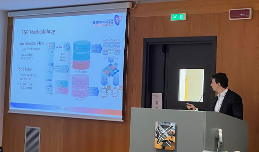
The two papers published in European Solid-State Circuits (ESSCIRC 2022) and International Conference on Computer-Aided Design (ICCAD 2022) are a preliminary result of the framework’s capabilities. The ICCAD 2022 paper details the chip design methodology tailored for ESP. The ESSCIRC 2022 paper applies the ESP framework with the new methodology to design a domain-specific SoC (DSSoC) for swarm-based perception applications (autonomous vehicle applications).
As far as I know, no other design methodology at the moment can implement a chip starting from PDK installation in four months. Moreover, no other methodology showed significant scalability between one chip and another without a time span penalty.
Finally, the complete ESP framework offers the user not only an agile, user-friendly physical design but also a methodology for accelerator design, a push button SoC integration capable of booting Linux OS, and chip testing support. In summary, ESP offers a complete agile design methodology starting from Linux software application, passing through a high-level language such as SystemC, C, Pytorch, and Tensor Flow, to mention but a few, to the final GDS file that is sent to chip fabrication.
Of course, there is space for improvement – and research – in the methodology on several fronts. Our main goal is to achieve an agile push button optimized physical design that keeps the main characteristics this methodology already has: flexibility, robustness, and scalability.
Q: Did anything surprise you about the research or the project?
From the beginning, I was always surprised regarding the project and research deliveries from the team. I am a very conservative and cautious person with respect to chip design. The ambition and increasing complexity of the project over time always concerned me. Therefore, at every milestone we achieved, I was impressed by what an engaged small talented team could do in such a short period!
Q: Can you talk about your background and why you pursued a PhD?
Before my PhD, I worked in chip design for 11 years. During this period, I taught how to design chips for a Brazilian government project in partnership with Cadence. This project aimed to increase the number of engineers in the country with the necessary knowledge and training to do chip design. I also designed chips and led a team to develop the RTL design flow at CEITEC, a Brazilian state-own semiconductor company.
I took my master’s while working, and at one point, I felt my career was at a plateau, and I wanted to do and learn different things. The PhD path started to sound perfect for me, especially when I could do it in the United States (US). Even though a PhD program in the US takes longer than in other countries, it is usually attached to some companies with daring projects. Therefore, it doesn’t detach you entirely from the industry, and it is easier to visualize a real-world application of your research. In addition, I would have the opportunity to use what I know, expand my knowledge, and learn important mainstream fields, such as machine learning.
Q: What are your research interests? How did you decide to pursue this type of research?
I have always liked to find ways to optimize processes. When it comes to chip design, a set of NP-Hard problems, the goal is to find improvements in the final result, which indicates you are in the right direction to a near-optimal solution.
Until recently, design problems relied on analytic algorithm solvers for design automation. Nowadays, the use of machine learning to predict and find chip design solutions is showing promising results in several stages of the design process. Therefore, focusing my research on chip design methodology that leverages algorithms and machine learning allows me to learn these topics and apply this new knowledge to optimize processes in a field I am already used to–chip design.
Q: What sort of research questions do you hope to answer?
Although we now have a flexible, robust, and scalable methodology, it is neither a push-button solution nor presents near-optimal results in terms of performance, power, and area. Therefore, my research focus now is to find ways to automate the still-required manual steps and, at the same time, produce near-global optimum solutions.
Q: What do you think is the most interesting thing about doing research?
Can I say two things? The first is the feeling that you are at the leading edge of some technology–the frontier between the known and unknown. The second is that you are not alone; other researchers are trying to find similar answers and are willing to collaborate.
Q: What are you working on now?
I am organizing the ESP ASIC design flow database to make it user-friendly and easy to maintain as we add support for new technologies, electronic design automation (EDA) tools, and ESP architecture features. Simultaneously, I am building a flow to easily port ESP RTL architecture from FPGA-ready prototyping to ASIC-ready prototyping and reading many chip design flow-related papers.
Q: What has been the highlight of your time at Columbia?
The research team I have been working with is all talented, hardworking people who do not hesitate to help each other. At the same time, whenever work allows, they are always down for having fun together as a team. This makes the PhD journey enjoyable and creates a bond that lasts beyond our time in Columbia.
Q: What is your advice to students on how to navigate their time at Columbia? If they want to do research, what should they know or do to prepare?
First, I would say don’t start a PhD without clear reasons. You don’t need to know what specific topic you would like to research, but you need to understand why you want a PhD and why now. The reason should not be driven by the money a PhD degree can provide alone.
After you have clear reasons, try to find some fields you are interested in and which professors can best guide you in each of these fields. The researcher’s daily life involves a lot of paper reading, nights and weekends of experiments (not all will have the expected results), and, sometimes, paper rejections. Be prepared for that and keep moving forward; your work will be recognized eventually.
Finally, get to know the research team you will be working with. You will spend a lot of your time with them – the joy of your journey is strongly attached to the people surrounding you!